Using Physics to Access the Silkscreen of a Printed Circuit Board

Discovery & Impact
Our customer wanted to research whether a circuit board coated in epoxy potting is an effective security measure to protect against reverse engineering attacks on printed circuit boards. The goal in this research was to be able to see silkscreen markings and map out component locations on the circuit board. We used a temperature attack based on the simple physics principle that materials will shrink at different rates when they are cooled past a certain degree. In this case, the fiberglass PCB will shrink at a different rate than epoxy, thus creating a separation between the two. By using liquid nitrogen, we were able to weaken the adhesion of the epoxy and eventually separate it from the circuit board, giving access to the (mirrored) silkscreen embedded in the epoxy.
Remediation Outcome
The conclusion of this research is that epoxy alone is not a sufficient security control against reverse engineering attacks. Appropriate security controls include removing any unnecessarily informational silkscreen markings such as those indicating critical components, ensuring that critical components, such as microcontrollers and flash, have read and write protections enabled, encrypt firmware, and add a layer of resistive foil or similar as a tamper measure to ensure that the device won’t function if an attacker drills through the epoxy to access components.
First, we acquired liquid nitrogen from a local welding supply store.
The liquid nitrogen made the epoxy's adhesion to the board more brittle, so we had to work delicately applying enough force to widen the crack and allow more nitrogen in but not so much force as to break the epoxy.
Little by little we were able to use scraping and pry tools to separate the epoxy from the circuit board into two pieces.
Almost the entire silkscreen layer came off of the PCB, but with the help of a black light and a bit of sandpaper we were able to see the (mirrored) silkscreen embedded in the epoxy.
Many/most of the components were ripped off the PCB, but the solder pads were still there, and we were able to trace the pins of the microcontroller to the debug headers.
Ultimately, we were able to show that even if the de-potted sample was destroyed in the process of removing the epoxy that an attacker would be able to see information such as silkscreen markings, general circuit layout, and the details and locations of critical components.
 Pew Pew, Precisely: The Physics and Practices Behind RayV Lite
 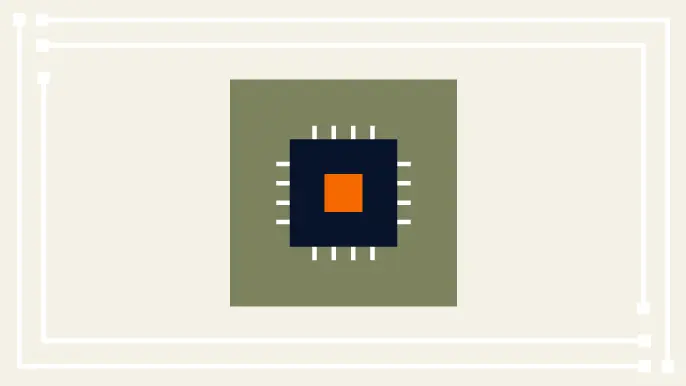 Practical Methods for Decapping Chips
  Fake It Until You Make It: Using Deep Fakes to Bypass Voice Biometrics